Enabling Google App Signing for Android Project

Signing key management of Android Apps is a hectic procedure and can grow out of hand rather quickly for large organizations with several independent projects. We, at FOSSASIA also had to face similar difficulties in management of individual keys by project maintainers and wanted to gather all these Android Projects under singular key management platform:

To handle the complexities and security aspect of the process, this year Google announced App Signing optional program where Google takes your existing key’s encrypted file and stores it on their servers and asks you to create a new upload key which will be used to sign further updates of the app. It takes the certificates of your new upload key and maps it to the managed private key. Now, whenever there is a new upload of the app, it’s signing certificate is matched with the upload key certificate and after verification, the app is signed by the original private key on the server itself and delivered to the user. The advantage comes where you lose your key, its password or it is compromised. Before App Signing program, if your key got lost, you had to launch your app under a new package name, losing your existing user base. With Google managing your key, if you lose your upload key, then the account owner can request Google to reassign a new upload key as the private key is secure on their servers.

There is no difference in the delivered app from the previous one as it is still finally signed by the original private key as it was before, except that Google also optimizes the app by splitting it into multiple APKs according to hardware, demographic and other factors, resulting in a much smaller app! This blog will take you through the steps in how to enable the program for existing and new apps. A bit of a warning though, for security reasons, opting in the program is permanent and once you do it, it is not possible to back out, so think it through before committing.

For existing apps:

First you need to go to the particular app’s detail section and then into Release Management > App Releases. There you would see the Get Started button for App Signing.

The account owner must first agree to its terms and conditions and once it’s done, a page like this will be presented with information about app signing infrastructure at top.

So, as per the instructions, download the PEPK jar file to encrypt your private key. For this process, you need to have your existing private key and its alias and password. It is fine if you don’t know the key password but store password is needed to generate the encrypted file. Then execute this command in the terminal as written in Step 2 of your Play console:

java -jar pepk.jar –keystore={{keystore_path}} –alias={{alias}} –output={{encrypted_file_output_path}} –encryptionkey=eb10fe8f7c7c9df715022017b00c6471f8ba8170b13049a11e6c09ffe3056a104a3bbe4ac5a955f4ba4fe93fc8cef27558a3eb9d2a529a2092761fb833b656cd48b9de6a

You will have to change the bold text inside curly braces to the correct keystore path, alias and the output file path you want respectively.

Note: The encryption key has been same for me for 3 different Play Store accounts, but might be different for you. So please confirm in Play console first

When you execute the command, it will ask you for the keystore password, and once you enter it, the encrypted file will be generated on the path you specified. You can upload it using the button on console.

After this, you’ll need to generate a new upload key. You can do this using several methods listed here, but for demonstration we’ll be using command line to do so:

keytool -genkey -v -keystore {{keystore_path}} -alias {{alias_name}} -keyalg RSA -keysize 2048 -validity 10000

The command will ask you a couple of questions related to the passwords and signing information and then the key will be generated. This will be your public key and be used for further signing of your apps. So keep it and the password secure and handy (even if it is expendable now).

After this step, you need to create a PEM upload certificate for this key, and in order to do so, execute this command:

keytool -export -rfc -keystore {{keystore_path}} -alias {{alias_name}} -file {{upload_certificate.pem}}

After this is executed, it’ll ask you the keystore password, and once you enter it, the PEM file will be generated and you will have to upload it to the Play console.

If everything goes right, your Play console will look something like this:


Click enrol and you’re done! Now you can go to App Signing section of the Release Management console and see your app signing and new upload key certificates


You can use the SHA1 hash to confirm the keys as to which one corresponds to private and upload if ever in confusion.

For new apps:

For new apps, the process is like a walk in park. You just need to enable the App Signing, and you’ll get an option to continue, opt-out or re-use existing key.


If you re-use existing key, the process is finished then and there and an existing key is deployed as the upload key for this app. But if you choose to Continue, then App Signing will be enabled and Google will use an arbitrary key as private key for the app and the first app you upload will get its key registered as the upload key


This is the screenshot of the App Signing console when there is no first app uploaded and you can see that it still has an app signing certificate of a key which you did not upload or have access to.

If you want to know more about app signing program, check out these links:

Continue ReadingEnabling Google App Signing for Android Project

How Switch Case improve performance in PSLab Saved Experiments

PSLab android application contains nearly 70 experiments one can experiment on using the PSLab device and the other necessary circuit components and devices. These experiments span over areas such as Electronics, Electrical, Physical and High school level. All these experiments are accessible via an android adapter in the repository named “PerformExperimentAdapter”. This adapter houses a tab view with two different tabs; one for the experiment details and the other for actual experiment and resultant graphs.

The adapter extends an inbuilt class FragmentPagerAdapter;

public class PerformExperimentAdapter extends FragmentPagerAdapter

This class displays every page attached to its viewpager as a fragment. The good thing about using fragments is that they have a recyclable life cycle. Rather than creating new views for every instance of an experiment, the similar views can be recycled to use once again saving resources and improving performance. FragmentPagerAdapter needs to override a method to display the correct view on the tab select by user.

@Override
public Fragment getItem(int position) {

}

Depending on the value of position, relevant experiment documentation and the experiment implementation fragments are displayed determined using the experiment title. Performance can be critical in this place as if it takes too long to process and render a fragment, user will feel a lag.

The previous implementation was using consecutive if statements.

@Override
public Fragment getItem(int position) {
   switch (position) {
       case 0:
           if (experimentTitle.equals(context.getString(R.string.diode_iv)))
               return ExperimentDocFragment.newInstance("D_diodeIV.html");
           if (experimentTitle.equals(context.getString(R.string.zener_iv)))
               return ExperimentDocFragment.newInstance("D_ZenerIV.html");
           ...
       case 1:
           if (experimentTitle.equals(context.getString(R.string.diode_iv)))
               return ZenerSetupFragment.newInstance();
           if (experimentTitle.equals(context.getString(R.string.zener_iv)))
               return DiodeExperiment.newInstance(context.getString(R.string.half_wave_rectifier));
           ...
       default:
           return ExperimentDocFragment.newInstance("astable-multivibrator.html");
   }
}

This setup was suitable for applications where there is less than around 5 choices to chose between. As the list grows, the elements in the end of the if layers will take more time to load as each of the previous if statements need to be evaluated false in order to reach the bottom statements.

This is when this implementation was replaced using switch case statements instead of consecutive if statements. The theory behind the performance improvement involves algorithm structures; Hash Tables

Hash Tables

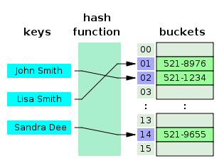
Hash tables use a hash function to calculate the index of the destination cell. This operation on average has a complexity of O(1) which means it will take the same time to access any two elements which are randomly positioned.

This is possible because java uses the hash code of the string to determine the index where the target is situated at. This way it is much faster than consecutive if statement calls where in the worst case it will take O(n) time to reach the statement causing a lag in the application.

Current application uses switch cases in the PerformExperimentAdapter;

@Override
public Fragment getItem(int position) {
   switch (position) {
       case 0:
           switch (experimentTitle) {
               case "Diode IV Characteristics":
                   return ExperimentDocFragment.newInstance("D_diodeIV.html");
               case "Zener IV Characteristics":
                   return ExperimentDocFragment.newInstance("D_ZenerIV.html");
               case "Half Wave Rectifier":
                   return ExperimentDocFragment.newInstance("L_halfWave.html");
           }
       case 1:
           switch (experimentTitle) {
               case "Diode IV Characteristics":
                   return ZenerSetupFragment.newInstance();
               case "Zener IV Characteristics":
                   return ZenerSetupFragment.newInstance();
               case "Half Wave Rectifier":
                   return DiodeExperiment.newInstance(context.getString(R.string.half_wave_rectifier));
           }
       default:
           return ExperimentDocFragment.newInstance("astable-multivibrator.html");
   }
}

There is one downfall in using switch case in the context. That is the inability to use string resources directly as Java requires a constant literals in the evaluation statement of a case.

Resources:

Continue ReadingHow Switch Case improve performance in PSLab Saved Experiments

Coloring Waveforms in PSLab Charts

Charts are used to display set of data in an analytical manner such that an observer can easily come to a conclusion by just looking at it without having to go through all the numerical data sets. Legends are used to differentiate a set of data set from another set. Generally, different colors and different names are used to form a legend in a chart.

MPAndroidChart is an amazing library with the capability of generating different types of graphs in an Android device. In PSLab several user interfaces are implemented using LineCharts to display different waveforms such as readings from channels attached to PSLab device, logic levels etc.

When several data sets are being plotted on the same graph area, legends are used. In PSLab Android application, Oscilloscope supports four different type of waveforms to be plotted on the same graph. Logic Analyzer implements one to four different types of logic level waveforms on the same plot. To identify which is which, legends with different colors can be used rather than just the names. For the legends to have different colors, it should be explicitly set which color should be held by which data set. Otherwise it will use the default color to all the legends making it hard to differentiate data lines when there are more than one data set is plotted.

Assume a data set is generated from a reading taken from a probe attached to PSLab device. The set will be added as an Entry to an array list as follows;

ArrayList<Entry> dataSet = new ArrayList<Entry>();

The next step will be to create a Line Data Set

LineDataSet lineData = new LineDataSet(dataSet, "DataSet 1");

This LineDataSet will contain sample values of the waveform captured by the microprocessor. A LineDataSet object support many methods to alter its look and feel. In order to set a color for the legend, setColor() method will be useful. This method accepts an integer as the color. This method can be accessed as follows;

lineData.setColor(Color.YELLOW);

MPAndroidChart provides different sets of colors under ColorTemplate. This class has several predefined colors with five colors in each color palette are added by the developers of the library and they can be accessed using the following line of code by simply calling the index value of the palette array list.

set1.setColor(ColorTemplate.JOYFUL_COLORS[0]);

Set of color palettes available in the ColorTemplate class are;

  1. LIBERTY_COLORS
  2. JOYFUL_COLORS
  3. PASTEL_COLORS
  4. COLORFUL_COLORS
  5. VORDIPLOM_COLORS
  6. MATERIAL_COLORS

The following demonstrates how the above activities produce a line chart with three different data sets with different colored legends.

This implementation can be used to enhance the readability of the waveforms letting user being able to differentiate between one waveform from another in PSLab Android application.

Resources:

PSLab official web site: https://pslab.fossasia.org/

Continue ReadingColoring Waveforms in PSLab Charts

Preparing for Automatic Publishing of Android Apps in Play Store

I spent this week searching through libraries and services which provide a way to publish built apks directly through API so that the repositories for Android apps can trigger publishing automatically after each push on master branch. The projects to be auto-deployed are:

I had eyes on fastlane for a couple of months and it came out to be the best solution for the task. The tool not only allows publishing of APK files, but also Play Store listings, screenshots, and changelogs. And that is only a subset of its capabilities bundled in a subservice supply.

There is a process before getting started to use this service, which I will go through step by step in this blog. The process is also outlined in the README of the supply project.

Enabling API Access

The first step in the process is to enable API access in your Play Store Developer account if you haven’t done so. For that, you have to open the Play Dev Console and go to Settings > Developer Account > API access.

If this is the first time you are opening it, you’ll be presented with a confirmation dialog detailing about the ramifications of the action and if you agree to do so. Read carefully about the terms and click accept if you agree with them. Once you do, you’ll be presented with a setting panel like this:

Creating Service Account

As you can see there is no registered service account here and we need to create one. So, click on CREATE SERVICE ACCOUNT button and this dialog will pop up giving you the instructions on how to do so:

So, open the highlighted link in the new tab and Google API Console will open up, which will look something like this:

Click on Create Service Account and fill in these details:

Account Name: Any name you want

Role: Project > Service Account Actor

And then, select Furnish a new private key and select JSON. Click CREATE.

A new JSON key will be created and downloaded on your device. Keep this secret as anyone with access to it can at least change play store listings of your apps if not upload new apps in place of existing ones (as they are protected by signing keys).

Granting Access

Now return to the Play Console tab (we were there in Figure 2 at the start of Creating Service Account), and click done as you have created the Service Account now. And you should see the created service account listed like this:

Now click on grant access, choose Release Manager from Role dropdown, and select these PERMISSIONS:

Of course you don’t want the fastlane API to access financial data or manage orders. Other than that it is up to you on what to allow or disallow. Same choice with expiry date as we have left it to never expire. Click on ADD USER and you’ll see the Release Manager created in the user list like below:

Now you are ready to use the fastlane service, or any other release management service for that matter.

Using fastlane

Install fastlane by

sudo gem install fastlane

Go to your project folder and run

fastlane supply init

First it will ask the location of the private key JSON file you downloaded, and then the package name of the application you are trying to initialize fastlane for.

Then it will create metadata folder with listing information excluding the images. So you’ll have to download and place the images manually for the first time

After modifying the listing, images or APK, run the command:

fastlane supply run

That’s it. Your app along with the store listing has been updated!

This is a very brief introduction to the capabilities of the supply service. All interactive options can be supplied via command line arguments, certain parts of the metadata can be omitted and alpha beta management along with release rollout can be done in steps! Make sure to check out the links below:

Continue ReadingPreparing for Automatic Publishing of Android Apps in Play Store

Fascinating Experiments with PSLab

PSLab can be extensively used in a variety of experiments ranging from the traditional electrical and electronics experiments to a number of innovative experiments. The PSLab desktop app and the Android app have all the essential features that are needed to perform the experiments. In addition to that there is a large collection of built-in experiments in both these experiments.

This blog is an extension to the blog post mentioned here. This blog lists some of the basic electrical and electronics experiments which are based on the same principles which are mentioned in the previous blog. In addition to that, some interesting and innovative experiments where PSLab can be used are also listed here. The experiments mentioned here require some prerequisite knowledge of electronic elements and basic circuit building. (The links mentioned at the end of the blog will be helpful in this case)

Op-Amp as an Inverting and a Non-Inverting Amplifier

There are two methods of doing this experiment. PSLab already has a built-in experiment dedicated to inverting and non-inverting amplification of op-amps. In the Android App, just navigate to Saved Experiments -> Electronics Experiments -> Op-Amp Circuits -> Inverting/ Non-Inverting. In case of the Desktop app, select Electronics Experiments from the main drop-down at the top of the window and select the Inverting/Non-inverting op-amp experiment.

This experiment can also performed using the basic features of PSLab. The only advantage of this methodology is that it allows much more tweaking of values to observe the Op-Amp behaviour in greater detail. However, the built-in experiment is good enough for most of the cases.

  • Construct the above circuits on a breadboard.
  • For the amplifier, connect the terminals of CH1 and GND of PSLab on the input side i.e. next to Vi and the terminals of CH2 and GND on the output side i.e next to Vo.
  • Usually, an Op-Amp like LM741 have a set of pins, one dedicated for the inverting input and the other dedicated for the non-inverting input. It is recommended to consult the datasheet of the Op-Amp IC used in order to get the pin number with which the input has to be connected.
  • The terminals of W1 and GND are also connected on the input side and they are used to generate a sine wave.
  • The resistors displayed in the figure have the values R1 = 10k and R2 = 51k. Resistance values other than these can also be considered. The gain of the op-amp would depend on the ratio of R2/R1, so it is better to consider values of R2 which are significantly larger than R1 in order to see the gain properly.
  • Use the PSLab Desktop App and open the Waveform Generator in Control. Set the wave type of W1 to Sine and set the frequency at 1 kHz and magnitude to 0.1 V. Then go ahead and open the Oscilloscope.
  • CH1 would display the input waveform and CH2 will display the output waveform and the plots can be observed.
  • If the input is connected to the inverting pin of the op-amp, the output obtained will be amplified and will have a phase difference of 90o with the input waveform whereas when the non-inverting pin is selected, the output is just amplified and no such phase difference is observed.
  • Note: Take proper care while connecting the V+ and V- pins of the op-amp, else the op-amp will be damaged.

Diode as an Integrator and Differentiator

An integrator in measurement and control applications is an element whose output signal is the time integral of its input signal. It accumulates the input quantity over a defined time to produce a representative output.

Integration is an important part of many engineering and scientific applications. Mechanical integrators are the oldest application, and are still used in such as metering of water flow or electric power. Electronic analogue integrators are the basis of analog computers and charge amplifiers. Integration is also performed by digital computing algorithms.

In electronics, a differentiator is a circuit that is designed such that the output of the circuit is approximately directly proportional to the rate of change (the time derivative) of the input. An active differentiator includes some form of amplifier. A passive differentiator circuit is made of only resistors and capacitors.

  • Construct the above circuits on a breadboard.
  • For both the circuits, connect the terminals of CH1 and GND of PSLab on the input side i.e. next to input voltage source and the terminals of CH2 and GND on the output side i.e next to Vo.
  • Ensure that the inverting and the non-inverting terminals of the op-amp are connected correctly. Check for the +/- signs in the diagram. ‘+’ corresponds to non-inverting and ‘-’ corresponds to inverting.
  • The terminals of W1 and GND are also connected on the input side and they are used to generate a sine wave.
  • The resistors displayed in the figure have the values R1 = 10k and R2 = 51k. Resistance values other than these can also be considered. The gain of the op-amp would depend on the ratio of R2/R1, so it is better to consider values of R2 which are significantly larger than R1 in order to see the gain properly.
  • Use the PSLab Desktop App and open the Waveform Generator in Control. Set the wave type of W1 to Sine and set the frequency at 1 kHz and magnitude to 5V (10V peak to peak). Then go ahead and open the Oscilloscope.
  • CH1 would display the input waveform and CH2 will display the output waveform and the plots can be observed.
  • If all the connections are made properly and the values of the parameters are set properly, then the waveform obtained should be as shown below.

Performing experiments involving ICs (Digital circuits)

The experiments mentioned so far including the ones mentioned in the previous blog post involved analog circuits and so they required features like the arbitrary waveform generator. However, digital circuits work using discrete values only. PSLab has the features needed to perform digital experiments which mainly involve the use of a square wave generator with a variable duty cycle.

PSLab board has dedicated pins named SQR1, SQR2, SQR3 and SQR4. The options for configuring these pins is present under the Advanced Control section in the Desktop app and in the Android app Applications->Control->Advanced. The options include selecting the pins which we want to use for digital outputs and then configuring the frequency and duty cycle of the square wave generated from that particular pin.

Innovative Experiments using PSLab

PSLab has quite a good number of interesting built-in experiments. These experiments can be found in the dropdown list at the top in the Desktop App and under the Saved Experiments header in the Android App. The built-in experiments come bundled with good quality documentation having circuit diagrams and detailed procedure to perform the experiments.

Some of the interesting experiments include:

  • Lemon Cell Experiment: In this experiment, the internal resistance and the voltage supplied by the lemon cell are measured.


  • Sound Beats: In acoustics, a beat is an interference pattern between two sounds of slightly different frequencies, perceived as a periodic variation in volume whose rate is the difference of the two frequencies.


  • When tuning instruments that can produce sustained tones, beats can readily be recognized. Tuning two tones to a unison will present a peculiar effect: when the two tones are close in pitch but not identical, the difference in frequency generates the beating.
  • This experiment requires producing two waves together of different frequencies and connecting them to the same oscilloscope channel. The pattern observed is shown below.

References:

  1. The previous blog on experiments using PSLab – https://blog.fossasia.org/electronics-experiments-with-pslab/
  2. More about op-amps and their characteristics – http://www.electronics-tutorials.ws/opamp/opamp_1.html
  3. Read more about differential and integrator circuits – https://www.allaboutcircuits.com/textbook/semiconductors/chpt-8/differentiator-integrator-circuits/
  4. Experiments involving digital circuits for reference – http://web.iitd.ac.in/~shouri/eep201/experiments.php

Continue ReadingFascinating Experiments with PSLab

Basics behind school level experiments with PSLab

Electronics is a fascinating subject to most kids. Turning on a LED bulb, making a simple circuit will make them dive into much more interesting areas in the field of electronics. PSLab android application with the help of PSLab device implements a set of experiments whose target audience is school children. To make them more interested in science and electronics, there are several experiments implemented such as measuring body resistance, lemon cell experiment etc.

This blog post brings out the basics in implementing these type of experiments and pre-requisite.

Lemon Cell Experiment

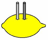
Lemon Cell experiment is a basic experiment which will make school kids interested in science experiments. The setup requires a fresh lemon and a pair of nails which is used to drive into the lemon as illustrated in the figure. The implementation in PSLab android application uses it’s Channel 1. The cell generates a low voltage which can be detected using the CH1 pin of PSLab device and it is sampled at a rate of 10 to read an accurate result.

float voltage = (float) scienceLab.getVoltage("CH1", 10);

2000 instances are recorded using this method and plotted against each instance. The output graph will show a decaying graph of voltage measured between the nails driven into the lemon.

for (int i = 0; i < timeAxis.size(); i++) {
   temp.add(new Entry(timeAxis.get(i), voltageAxis.get(i)));
}

Human Body Resistance Measurement Experiment

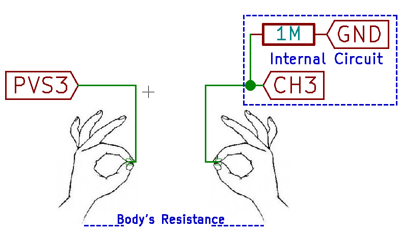
This experiment attracts most of the young people to do electronic experiments. This is implemented in the PSLab android application using Channel 3 and the Programmable Voltage Source 3 which can generate voltage up to 3.3V. The experiment requires a human with drippy palms so it makes a good conductance between device connection and the body itself.

The PSLab device has an internal resistance of 1M Ohms connected with the Channel 3 pin. Experiment requires a student to hold two wires with the metal core exposed; in both hands. One wire is connected to PV3 pin when the other wire is connected to CH3 pin. When a low voltage is supplied from the PV3 pin, due to heavy resistance in body and the PSLab device, a small current in the range of nano amperes will flow through body. Using the reading from CH3 pin and the following calculation, body resistance can be measured.

voltage = (float) scienceLab.getVoltage("CH3", 100);
current = voltage / M;
resistance = (M * (PV3Voltage - voltage)) / voltage;

This operation is executed inside a while loop to provide user with a continuous set of readings. Using Java threads there is a workaround to implement the functionalities inside the while loop without overwhelming the system. First step is to create a object without any attribute.

private final Object lock = new Object();

Java threads use synchronized methods where other threads won’t start until the first thread is completed or paused operation. We make use of that technique to provide enough time to read CH3 pin and display output.

while (true) {
   new MeasureResistance().execute();
   synchronized (lock) {
       try {
           lock.wait();
       } catch (InterruptedException e) {
           e.printStackTrace();
       }
   }
}

Once the pin readings and value updates are complete the lock is released to execute the method once again.

updateDataBox();
synchronized (lock) {
   lock.notify();
}

Capacitor Discharge Experiment

This experiment is somewhat similar to the Lemon Cell Experiment as this experiments on electron storage and discharge. The experiment is carried out using two bulky electrolyte capacitors. PSLab device is capable of generating PWM waveforms with any duty cycle. Refer to this article to learn more about how PWM waves are generated using PSLab device to implement more features like sine wave generation.

Using the SQR1 pin of the PSLab device, one capacitor is charged to its fullest capacity using a PWM wave with 100% duty cycle at a 100 Hz.

scienceLab.setSqr1(100, 100, false);

This capacitor is then connected in parallel with the other capacitor which is empty. The voltage transfer is measured using CH1 pin at a sampling rate of 10

float voltage = (float) scienceLab.getVoltage("CH1", 10);

To provide a continuous update in the voltage transfer, a similar implementation is used using an object in the thread to control the implementation inside a while loop.

Resources:

Continue ReadingBasics behind school level experiments with PSLab

Implement Wave Generation Functionality in The PSLab Android App

The PSLab Android App works as an Oscilloscope using the audio jack of Android device. The implementation for the scope using in-built mic is discussed in the post Using the Audio Jack to make an Oscilloscope in the PSLab Android App. Another application which can be implemented by hacking the audio jack is Wave Generation. We can generate different types of signals on the wires connected to the audio jack using the Android APIs that control the Audio Hardware. In this post, I will discuss about how we can generate wave by using the Android APIs for controlling the audio hardware.

Configuration of Audio Jack for Wave Generation

Simply cut open the wire of a cheap pair of earphones to gain control of its terminals and attach alligator pins by soldering or any other hack(jugaad) that you can think of. After you are done with the tinkering of the earphone jack, it should look something like shown in the image below.

Source: edn.com

If your earphones had mic, it would have an extra wire for mic input. In any general pair of earphones the wire configuration is almost the same as shown in the image below.

Source: flickr

Android APIs for Controlling Audio Hardware

AudioRecord and AudioTrack are the two classes in Android that manages recording and playback respectively. For Wave Generation application we only need AudioTrack class.

Creating an AudioTrack object: We need the following parameters to initialise an AudioTrack object.

STREAM TYPE: Type of stream like STREAM_SYSTEM, STREAM_MUSIC, STREAM_RING, etc. For wave generation purpose we are using stream music. Every stream has its own maximum and minimum volume level.

SAMPLING RATE: it is the rate at which source samples the audio signal.

BUFFER SIZE IN BYTES: total size in bytes of the internal buffer from where the audio data is read for playback.

MODES: There are two modes

  • MODE_STATIC: Audio data is transferred from Java to native layer only once before the audio starts playing.
  • MODE_STREAM: Audio data is streamed from Java to native layer as audio is being played.

getMinBufferSize() returns the estimated minimum buffer size required for an AudioTrack object to be created in the MODE_STREAM mode.

private int minTrackBufferSize;
private static final int SAMPLING_RATE = 44100;
minTrackBufferSize = AudioTrack.getMinBufferSize(SAMPLING_RATE, AudioFormat.CHANNEL_OUT_MONO, AudioFormat.ENCODING_PCM_16BIT);

audioTrack = new AudioTrack(
       AudioManager.STREAM_MUSIC,
       SAMPLING_RATE,
       AudioFormat.CHANNEL_OUT_MONO,
       AudioFormat.ENCODING_PCM_16BIT,
       minTrackBufferSize,
       AudioTrack.MODE_STREAM);

Function createBuffer() creates the audio buffer that is played using the audio track object i.e audio track object would write this buffer on playback stream. Function below fills random values in the buffer due to which a random signal is generated. If we want to generate some specific wave like Square Wave, Sine Wave, Triangular Wave, we have to fill the buffer accordingly.

public short[] createBuffer(int frequency) {
   // generating a random buffer for now
   short[] buffer = new short[minTrackBufferSize];
   for (int i = 0; i < minTrackBufferSize; i++) {
       buffer[i] = (short) (random.nextInt(32767) + (-32768));
   }
   return buffer;
}

We created a write() method and passed the audio buffer created in above step as an argument to the method. This method writes audio buffer into audio stream for playback.

public void write(short[] buffer) {
   /* write buffer to audioTrack */
   audioTrack.write(buffer, 0, buffer.length);
}

Amplitude of the signal can be controlled by changing the volume level of the stream on which the buffer is being played. As we are playing the audio in music stream, so STREAM_MUSIC is passed as a parameter to the setStreamVolume() method.

value: value is amplitude level of the stream. Every stream has its different amplitude levels. getStreamMaxVolume(STREAM_TYPE) method is used to find the maximum valid amplitude level of any stream.
flag: this stackoverflow post explain all the flags of the AudioManager class.

AudioManager audioManager = (AudioManager)getSystemService(Context.AUDIO_SERVICE); audioManager.setStreamVolume(AudioManager.STREAM_MUSIC, value, flag);

Roadmap

We are working on implementing methods to fill audio buffer with specific values such that waves like Sinusoidal wave, Square Wave, Sawtooth Wave can be generated during the playback of the buffer using the AudioTrack object.

Resources

Continue ReadingImplement Wave Generation Functionality in The PSLab Android App

Basics behind BJT and FET experiments in PSLab

A high school student in his curriculum; will come across certain electronics and electrical experiments. One of them related to semiconductor devices such as Bipolar Junction Transistors (BJTs) and Field Effect Transistors (FETs). PSLab device is capable of function as a waveform generator, voltage and current source, oscilloscope and multimeter. Using these functionalities one can design an experiment. This blog post brings out the basics one should know about the experiment and the PSLab device to program an experiment in the saved experiments section.

Channels and Sources in the PSLab Device

The PSLab device has three pins dedicated to function as programmable voltage sources (PVS) and one pin for programmable current source (PCS).

Programmable Voltage Sources can generate voltages as follows;

  • PV1 →  -5V ~ +5V
  • PV2 → -3.3V ~ +3.3V
  • PV3 → 0 ~ +3.3V

Programmable Current Source (PCS) can generate current as follows;

  • PCS → 0 ~ 3.3mA

The device has 4 channel oscilloscope out of those CH1, CH2 and CH3 pins are useful in experiments of the current context type.

About BJTs and FETs

Every semiconductor device is made of Silicon(Si). Some are made of Germanium(Ge) but they are not widely used. Silicon material has a potential barrier of 0.7 V among P type and N type sections of a semiconductor device. This voltage value is really important in an experiment as in some practicals such as “BJT Amplifier”, there is no use of a voltage value setting below this value. So the experiment needs to be programmed to have 0.7V as the minimum voltage for Base terminal.

Basic BJT experiments

BJTs have three pins. Collector, Emitter and Base. Current to the Base pin will control the flow of electrons from Emitter to Collector creating a voltage difference between Collector and Emitter pins. This scenario can be taken down to three types as;

  • Input Characteristics → Relationship between Emitter current to VBE(Base to Emitter)
  • Output Characteristics → Relationship between IC(Collector) to VCB(Collector to Base)
  • Transfer Characteristics → Relationship between IC(Collector) to IE(Emitter)

Input Characteristics

Output Characteristics

Transfer Characteristics


Basic FET experiments

FETs have three pins. Drain, Source and Gate. Voltage to Gate terminal will control the electron flow from either direction from or to Source and Drain. This scenario results in two types of experiments;

  • Output Characteristics → Drain current to Drain to Source voltage difference
  • Transfer Characteristics → Gate to Source voltage to Drain current
Output Characteristics Transfer Characteristics

Using existing methods in PSLab android repository

Current implementation of the android application consists of all the methods required to read voltages and currents from the relevant pins and fetch waveforms from the channel pins and output voltages from PVS pins.

ScienceLab.java class – This class implements all the methods required for any kind of an experiment. The methods that will be useful in designing BJT and FET related experiments are;

Set Voltages

public void setPV1(float value);

public void setPV2(float value);

public void setPV3(float value);

Set Currents

public void setPCS(float value);

Read Voltages

public double getVoltage(String channelName, Integer sample);

Read Currents

To read current there is no direct way implemented. The current flow between two nodes can be calculated using the PVS pin value and the voltage value read from the channel pins. It uses Ohm’s law to calculate the value using the known resistance between two nodes.

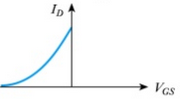
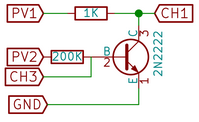
In the following schematic; the collector current can be calculated using known PV1 value and the measured CH1 value as follows;

IC = (PV1 – CH1) / 1000

This is how it is actually implemented in the existing experiments.

If one needs to implement a new experiment of any kind, these are the basics need to know. There can be so many new experiments implemented using these basics. Some of them could be;

  • Effect of Temperature coefficient in Collector current
  • The influence in β factor in Collector current

Resources:

Continue ReadingBasics behind BJT and FET experiments in PSLab

Electronics Experiments with PSLab

Numerous college level electronics experiments can be performed using Pocket Science Lab (PSLab). The Android app and the Desktop app have all the essential features needed to perform these experiments and both these apps have quite a large number of experiments built-in. Some of the common experiments involve the use of BJT (Bipolar Junction Transistor), Zener Diode, FET (Field Effect Transistor), Op-Amp ( Operational Amplifier) etc. This blog walks through the details of performing some experiments using the above commonly used elements.  

The materials required for all the experiments are minimal and includes a few things like PSLab hardware device, components like Diodes, Transistors, Op-Amps etc., connecting wires/jumpers and secondary components like resistors, capacitors etc. Most of these elements would be a part of the PSLab Accessory Kit.

It is recommended to read this blog here, go through the resources mentioned at the end and also get acquainted with construction of circuits before advancing with the experiments mentioned in this blog.

Half Wave and Full Wave Rectifiers

The Bipolar Junction Transistor (BJT) can be used as a rectifier. Rectifiers are needed in circuits to obtain a nearly constant and stable output voltage and prevent any ripples in the circuit. The rectifier can be half wave or full wave depending on whether it rectifies one or both cycles of Alternating Voltage.

The circuit for the Half and Full Wave rectifier is given as follows:

  • Construct the above circuits on a breadboard.
  • For the half wave rectifier, connect the terminals of CH1 and GND of PSLab on the input side and the terminals of CH2 and GND on the output side.
  • The terminals of W1 and GND are also connected on the input side and they are used to generate a sine wave.
  • Use the PSLab Desktop App and open the Waveform Generator in Control. Set the wave type of W1 to Sine and set the frequency at 100 Hz and magnitude to 10mV. Then go ahead and open the Oscilloscope.
  • CH1 would display the input waveform and CH2 will display the output waveform and the plots can be observed.
  • The plot obtained will have rectification in only half of the cycle. In order to obtain rectification in the complete cycle, the full wave rectifier is needed.
  • For the full wave rectifier, the procedure is the same but an additional diode is used. Use an additional channel CH3 to plot the extra input.

  • The plot obtained from the above steps would still have ripples and so a capacitor is placed in parallel to cancel this effect.
  • Place a 100uF/330uF capacitor in parallel to the resistor RL and an additional 1 ohm resistor in the circuit.

BJT Inverter

  • Transistor has a lot of functions. The most common of them is its use as an amplifier. However, transistor can be used as a switch in a circuit i.e. as an inverter.
  • The circuit for this experiment is shown below. For this experiment, it is recommended to use an external 5V DC supply like a battery. Connect the transistor and the diode initially and then connect the resistors accordingly. (Connect the terminals of diode and transistor carefully else they will be damaged).
  • When the circuit is constructed completely, connect CH1 to Vi and CH2 to Vo. Vi and Vo are input and outputs respectively and are marked in the figure.
  • The terminals of W1 and GND are also connected on the input side and they are used to generate a sine wave.
  • Use the PSLab Desktop App and open the Waveform Generator in Control. Set the wave type of W1 to Sine and set the frequency at 200 Hz and magnitude to 10mV.
  • Then go ahead and open the Oscilloscope. Use the X-Y mode of the oscilloscope to obtain the plot between Vi and Vo which should look like the graph shown below.

Common Mode Gain and Differential Mode Gain in Op-Amps

Gain of any amplifier can be calculated by calculating the ratio of the output and input voltage. On plotting the graph in X-Y mode, a Vo vs Vi graph is obtained. The slope of that graph gives us the gain at any particular input voltage.

  • For finding the Differential Mode gain of an Op-Amp, construct the circuit as shown below.
  • When the circuit is constructed completely, connect CH1 to Vi and CH2 to Vo. Vi and Vo are input and outputs respectively and are marked in the figure. The terminals of W1 and GND are also connected on the input side and they are used to generate a sine wave.
  • The power supply provided to the Op-Amp are set to + 12V. (If faced with any confusion, please refer to the resources mentioned at the end of the blog to learn more about Op-Amps before proceeding ahead.)
  • Use the PSLab Desktop App and open the Waveform Generator in Control. Set the wave type of W1 to Sine and set the frequency at 1000 Hz and magnitude to 0.5V. Then go ahead and open the Oscilloscope. Use the X-Y mode of the oscilloscope to obtain the plot between Vi and Vo.
  • For finding the Common Mode gain of the Op-Amp, remove the waveform generator input i.e W1 from R3 and attach it to R2. The rest of the steps remain the same.

Schmitt Trigger

In electronics, a Schmitt trigger is a comparator circuit with hysteresis implemented by applying positive feedback to the noninverting input of a comparator or differential amplifier. It is an active circuit which converts an analog input signal to a digital output signal.

  • Construct the circuit as shown below. Although the diagram shows a variable resistor be used, a constant value resistor would also work fine.
  • When the circuit is constructed completely, connect CH1 to Vi and CH2 to Vo. Vi and Vo are input and outputs respectively and are marked in the figure. The terminals of W1 and GND are also connected on the input side and they are used to generate a sine wave.
  • The power supply provided to the Op-Amp are set to + 12V. (If faced with any confusion, please refer to the resources mentioned at the end of the blog to learn more about Op-Amps before proceeding ahead. If done incorrectly, Op-Amps will be damaged)
  • Use the PSLab Desktop App and open the Waveform Generator in Control. Set the wave type of W1 to Sine and set the frequency at 1000 Hz and magnitude to 0.5V. Then go ahead and open the Oscilloscope. Use the X-Y mode of the oscilloscope to obtain the plot between Vi and Vo which should look like the graph shown below.

Resources:

  1. Read more about Half wave and Full wave rectifier and their applications – https://en.wikipedia.org/wiki/Rectifier
  2. Read more about the Bipolar Junction Transistor and its use as a switch – http://www.electronicshub.org/transistor-as-switch/
  3. Understand the common mode and differential mode of Op-Amp – https://www.allaboutcircuits.com/video-lectures/op-amps-common-differential/
  4. Find more about Schmitt Trigger and its uses – https://en.wikipedia.org/wiki/Schmitt_trigger

Continue ReadingElectronics Experiments with PSLab

SPI Communication in PSLab

PSLab supports communication using the Serial Peripheral Interface (SPI) protocol. The Desktop App as well as the Android App have the framework set-up to use this feature. SPI protocol is mainly used by a few sensors which can be connected to PSLab. For supporting SPI communication, the PSLab Communication library has a dedicated class defined for SPI. A brief overview of how SPI communication works and its advantages & limitations can be found here.

The class dedicated for SPI communication with numerous methods defined in them. The methods required for a particular SPI sensor may differ slightly, however, in general most sensors utilise a certain common set of methods. The set of methods that are commonly used are listed below with their functions.

In the setParameters method, the SPI parameters like Clock Polarity (CKP/CPOL), Clock Edge (CKE/CPHA), SPI modes (SMP) and other parameters like primary and secondary prescalar which are specific to the device used.

Primary Prescaler (0,1,2,3) for 64MHz clock->(64:1,16:1,4:1,1:1)

Secondary prescaler (0,1,..7)->(8:1,7:1,..1:1)

The values of CKP/CPOL and CKE/CPHA needs to set using the following convention and according to our requirements.

  • At CPOL=0 the base value of the clock is zero, i.e. the idle state is 0 and active state is 1.
    • For CPHA=0, data is captured on the clock’s rising edge (low→high transition) and data is changed at the falling edge (high→low transition).
    • For CPHA=1, data is captured on the clock’s falling edge (high→low transition) and data is changed at the rising edge (low→high transition).
  • At CPOL=1 the base value of the clock is one (inversion of CPOL=0), i.e. the idle state is 1 and active state is 0.
    • For CPHA=0, data is captured on the clock’s falling edge (high→low transition) and data is changed at the rising edge (low→high transition).
    • For CPHA=1, data is captured on the clock’s rising edge (low→high transition) and data is changed at the falling edge (high→low transition).

public void setParameters(int primaryPreScalar, int secondaryPreScalar, Integer CKE, Integer CKP, Integer SMP) throws IOException {
        if (CKE != null) this.CKE = CKE;
        if (CKP != null) this.CKP = CKP;
        if (SMP != null) this.SMP = SMP;

        packetHandler.sendByte(commandsProto.SPI_HEADER);
        packetHandler.sendByte(commandsProto.SET_SPI_PARAMETERS);
        packetHandler.sendByte(secondaryPreScalar | (primaryPreScalar << 3) | (this.CKE << 5) | (this.CKP << 6) | (this.SMP << 7));
        packetHandler.getAcknowledgement();
    }


The start method is responsible for sending the instruction to initiate the SPI communication and it takes the channel which will be used for communication as input.

public void start(int channel) throws IOException {
        packetHandler.sendByte(commandsProto.SPI_HEADER);
        packetHandler.sendByte(commandsProto.START_SPI);
        packetHandler.sendByte(channel);
    }


The setCS method is responsible for selecting the slave with which the SPI communication has to be done. This feature of SPI communication is known as Chip Select (CS) or Slave Select (SS). A master can use multiple Chip/Slave Select pins for communication whereas a slave utilises just one pin as SPI is based on single master multiple slaves principle. The capacity of PSLab is limited to two slave devices at a time.

public void setCS(String channel, int state) throws IOException {
        String[] chipSelect = new String[]{"CS1", "CS2"};
        channel = channel.toUpperCase();
        if (Arrays.asList(chipSelect).contains(channel)) {
            int csNum = Arrays.asList(chipSelect).indexOf(channel) + 9;
            packetHandler.sendByte(commandsProto.SPI_HEADER);
            if (state == 1)
                packetHandler.sendByte(commandsProto.STOP_SPI);
            else
                packetHandler.sendByte(commandsProto.START_SPI);
            packetHandler.sendByte(csNum);
        } else {
            Log.d(TAG, "Channel does not exist");
        }
    }


The stop method is responsible for sending the instruction to the stop the communication with the slave.

public void stop(int channel) throws IOException {
        packetHandler.sendByte(commandsProto.SPI_HEADER);
        packetHandler.sendByte(commandsProto.STOP_SPI);
        packetHandler.sendByte(channel);
    }


PSLab SPI class has methods defined for sending either 8-bit or 16-bit data over SPI which are further classified on whether they request the acknowledgement byte (it helps to know whether the communication was successful or unsuccessful) or not.

The methods are so named send8, send16, send8_burst and send16_burst . The burst methods do not request any acknowledgement value and as a result work faster than the normal methods.

public int send16(int value) throws IOException {
        packetHandler.sendByte(commandsProto.SPI_HEADER);
        packetHandler.sendByte(commandsProto.SEND_SPI16);
        packetHandler.sendInt(value);
        int retValue = packetHandler.getInt();
        packetHandler.getAcknowledgement();
        return retValue;
    }


Resources:

Continue ReadingSPI Communication in PSLab