Coloring Waveforms in PSLab Charts

Charts are used to display set of data in an analytical manner such that an observer can easily come to a conclusion by just looking at it without having to go through all the numerical data sets. Legends are used to differentiate a set of data set from another set. Generally, different colors and different names are used to form a legend in a chart.

MPAndroidChart is an amazing library with the capability of generating different types of graphs in an Android device. In PSLab several user interfaces are implemented using LineCharts to display different waveforms such as readings from channels attached to PSLab device, logic levels etc.

When several data sets are being plotted on the same graph area, legends are used. In PSLab Android application, Oscilloscope supports four different type of waveforms to be plotted on the same graph. Logic Analyzer implements one to four different types of logic level waveforms on the same plot. To identify which is which, legends with different colors can be used rather than just the names. For the legends to have different colors, it should be explicitly set which color should be held by which data set. Otherwise it will use the default color to all the legends making it hard to differentiate data lines when there are more than one data set is plotted.

Assume a data set is generated from a reading taken from a probe attached to PSLab device. The set will be added as an Entry to an array list as follows;

ArrayList<Entry> dataSet = new ArrayList<Entry>();

The next step will be to create a Line Data Set

LineDataSet lineData = new LineDataSet(dataSet, "DataSet 1");

This LineDataSet will contain sample values of the waveform captured by the microprocessor. A LineDataSet object support many methods to alter its look and feel. In order to set a color for the legend, setColor() method will be useful. This method accepts an integer as the color. This method can be accessed as follows;

lineData.setColor(Color.YELLOW);

MPAndroidChart provides different sets of colors under ColorTemplate. This class has several predefined colors with five colors in each color palette are added by the developers of the library and they can be accessed using the following line of code by simply calling the index value of the palette array list.

set1.setColor(ColorTemplate.JOYFUL_COLORS[0]);

Set of color palettes available in the ColorTemplate class are;

  1. LIBERTY_COLORS
  2. JOYFUL_COLORS
  3. PASTEL_COLORS
  4. COLORFUL_COLORS
  5. VORDIPLOM_COLORS
  6. MATERIAL_COLORS

The following demonstrates how the above activities produce a line chart with three different data sets with different colored legends.

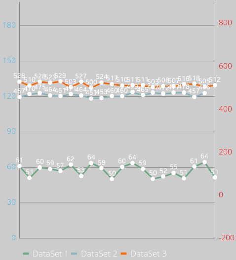
This implementation can be used to enhance the readability of the waveforms letting user being able to differentiate between one waveform from another in PSLab Android application.

Resources:

PSLab official web site: https://pslab.fossasia.org/

Continue ReadingColoring Waveforms in PSLab Charts

Performing Diode Clipping and Clamping Experiment in PSLab Android

We can perform experiments like diode clipping and clamping using PSLab Android. A circuit which removes the peak of a waveform is known as a clipper. Diode clipper cuts off the top half or lower half or both top and lower half of the input signal. 

Different types of clipping circuits listed below

Different Clipping Experiments

A clamper circuit adds the positive dc component to the input signal to push it to the positive side. Similarly, a clamper circuit adds the negative dc component to the input signal to push it to the negative side. It basically shifts the input signal without changing the shape of the signal.

Different Clamping Experiments

Apparatus

Diode, Resistance, Capacitor (only for diode clamping), Breadboard, Wires and PSLab

Adding Diode Clipping Experiment support in PSLab Android App

To support Diode Clipping Experiment we require generating a sine wave and a dc component. This can be done using W1 and PV1 pins in PSLab device. Both input and output signals can be read using CH1 and CH2. So, when the Diode Clipping Experiment needs to be performed the following code needs to be implemented

scienceLab.setSine1(5000);
scienceLab.setPV1(//progress of the seekbar);

The signals are recorded using Oscilloscope Activity.

Adding Diode Clamping Experiment support in PSLab Android App

Diode Clamping Experiment was implemented similarly to Diode Clipping Experiment. The following are the screenshots of the experiment.     

The following is a glimpse of Diode Clamping Experiment performed using PSLab device using PSLab Android App.

Resources

  1. Read more about Clipper Circuits –
  2. Read more information about Clamping Circuits –

Continue ReadingPerforming Diode Clipping and Clamping Experiment in PSLab Android

Sensor Data Logging in the PSLab Android App

The PSLab Android App allows users to log data from sensors connected to the PSLab hardware device. The Connected sensors should support I2C, SPI communication protocols to communicate with the PSLab device successfully. The only prerequisite is the additional support for the particular sensor plugin in Android App. The user can log data from various sensors and measure parameters like temperature, humidity, acceleration, magnetic field, etc. These parameters are useful in predicting and monitoring the environment and in performing many experiments.

The support for the sensor plugins was added during the porting python communication library code to Java. In this post,  we will discuss how we logged real time sensor data from the PSLab Hardware Device. We used Realm database to store the sensor data locally. We have taken the MPU6050 sensor as an example to understand the complete process of logging sensor data.

Creating Realm Object for MPU6050 Sensor Data

The MPU6050 sensor gives the acceleration and gyroscope readings along the three axes X, Y and Z. So the data object storing the readings of the mpu sensor have variables to store the acceleration and gyroscope readings along all three axes.

public class DataMPU6050 extends RealmObject {

   private double ax, ay, az;
   private double gx, gy, gz;
   private double temperature;

   public DataMPU6050() {  }

   public DataMPU6050(double ax, double ay, double az, double gx, double gy, double gz, double temperature) {
       this.ax = ax;
       this.ay = ay;
       this.az = az;
       this.gx = gx;
       this.gy = gy;
       this.gz = gz;
       this.temperature = temperature;
   }

  // getter and setter for all variables
}

Creating Runnable to Start/Stop Data Logging

To sample the sensor data at 500ms interval, we created a runnable object and passed it to another thread which would prevent lagging of the UI thread. We can start/stop logging by changing the value of the boolean loggingThreadRunning on button click. TaskMPU6050 is an AsyncTask which reads each sample of sensor data from the PSLab device, it gets executed inside a while loop which is controlled by boolean loggingThreadRunning. Thread.sleep(500) pauses the thread for 500ms, this is also one of the reason to transfer the logging to another thread instead of logging the sensor data in UI thread. If such 500ms delays are incorporated in UI thread, app experience won’t be smooth for the users.

Runnable loggingRunnable = new Runnable() {
   @Override
   public void run() {
       try {
           MPU6050 sensorMPU6050 = new MPU6050(i2c);
           while (loggingThreadRunning) {
               TaskMPU6050 taskMPU6050 = new TaskMPU6050(sensorMPU6050);
               taskMPU6050.execute();
              // use lock object to synchronize threads
               Thread.sleep(500);
           }
       } catch (IOException   InterruptedException e) {
           e.printStackTrace();
       }
   }
};

Sampling of Sensor Data

We created an AsyncTask to read each sample of the sensor data from the PSLab device in the background thread. The getRaw() method read raw values from the sensor and returned an ArrayList containing the acceleration and gyro values. After the values were read successfully, they were updated in the data card in the foreground which was visible to the user. This data card acts as a real-time screen for the user. All the samples read are appended to ArrayList mpu6050DataList, when the user clicks on button Save Data, the collected samples are saved to the local realm database.

private ArrayList<DataMPU6050> mpu6050DataList = new ArrayList<>();

private class TaskMPU6050 extends AsyncTask<Void, Void, Void> {

   private MPU6050 sensorMPU6050;
   private ArrayList<Double> dataMPU6050 = new ArrayList<>();

   TaskMPU6050(MPU6050 mpu6050) {
       this.sensorMPU6050 = mpu6050;
   }

   @Override
   protected Void doInBackground(Void... params) {
       try {
           dataMPU6050 = sensorMPU6050.getRaw();
       } catch (IOException e) {
           e.printStackTrace();
       }
       return null;
   }

   @Override
   protected void onPostExecute(Void aVoid) {
       super.onPostExecute(aVoid);
       // update data card TextViews with data read.
       DataMPU6050 tempObject = new DataMPU6050(dataMPU6050.get(0), dataMPU6050.get(1), dataMPU6050.get(2),
               dataMPU6050.get(4), dataMPU6050.get(5), dataMPU6050.get(6), dataMPU6050.get(3));
       mpu6050DataList.add(tempObject);
       synchronized (lock) {
           lock.notify();
       }
   }
}
Source: PSLab Android App

There is an option for Start/Stop Logging, clicking on which will change the value of boolean loggingThreadRunning which stops starts/stops the logging thread.

When the Save Data button is clicked, all the samples of sensor data collected from the  PSLab device till that point are saved to the local realm database.

realm.beginTransaction();
for (DataMPU6050 tempObject : mpu6050DataList) {
   realm.copyToRealm(tempObject);
}
realm.commitTransaction();

Data can also be written asynchronously to the local realm database. For other methods to write to a real database refer write section of Realm docs.

Resources

Continue ReadingSensor Data Logging in the PSLab Android App

Preparing for Automatic Publishing of Android Apps in Play Store

I spent this week searching through libraries and services which provide a way to publish built apks directly through API so that the repositories for Android apps can trigger publishing automatically after each push on master branch. The projects to be auto-deployed are:

I had eyes on fastlane for a couple of months and it came out to be the best solution for the task. The tool not only allows publishing of APK files, but also Play Store listings, screenshots, and changelogs. And that is only a subset of its capabilities bundled in a subservice supply.

There is a process before getting started to use this service, which I will go through step by step in this blog. The process is also outlined in the README of the supply project.

Enabling API Access

The first step in the process is to enable API access in your Play Store Developer account if you haven’t done so. For that, you have to open the Play Dev Console and go to Settings > Developer Account > API access.

If this is the first time you are opening it, you’ll be presented with a confirmation dialog detailing about the ramifications of the action and if you agree to do so. Read carefully about the terms and click accept if you agree with them. Once you do, you’ll be presented with a setting panel like this:

Creating Service Account

As you can see there is no registered service account here and we need to create one. So, click on CREATE SERVICE ACCOUNT button and this dialog will pop up giving you the instructions on how to do so:

So, open the highlighted link in the new tab and Google API Console will open up, which will look something like this:

Click on Create Service Account and fill in these details:

Account Name: Any name you want

Role: Project > Service Account Actor

And then, select Furnish a new private key and select JSON. Click CREATE.

A new JSON key will be created and downloaded on your device. Keep this secret as anyone with access to it can at least change play store listings of your apps if not upload new apps in place of existing ones (as they are protected by signing keys).

Granting Access

Now return to the Play Console tab (we were there in Figure 2 at the start of Creating Service Account), and click done as you have created the Service Account now. And you should see the created service account listed like this:

Now click on grant access, choose Release Manager from Role dropdown, and select these PERMISSIONS:

Of course you don’t want the fastlane API to access financial data or manage orders. Other than that it is up to you on what to allow or disallow. Same choice with expiry date as we have left it to never expire. Click on ADD USER and you’ll see the Release Manager created in the user list like below:

Now you are ready to use the fastlane service, or any other release management service for that matter.

Using fastlane

Install fastlane by

sudo gem install fastlane

Go to your project folder and run

fastlane supply init

First it will ask the location of the private key JSON file you downloaded, and then the package name of the application you are trying to initialize fastlane for.

Then it will create metadata folder with listing information excluding the images. So you’ll have to download and place the images manually for the first time

After modifying the listing, images or APK, run the command:

fastlane supply run

That’s it. Your app along with the store listing has been updated!

This is a very brief introduction to the capabilities of the supply service. All interactive options can be supplied via command line arguments, certain parts of the metadata can be omitted and alpha beta management along with release rollout can be done in steps! Make sure to check out the links below:

Continue ReadingPreparing for Automatic Publishing of Android Apps in Play Store

Fascinating Experiments with PSLab

PSLab can be extensively used in a variety of experiments ranging from the traditional electrical and electronics experiments to a number of innovative experiments. The PSLab desktop app and the Android app have all the essential features that are needed to perform the experiments. In addition to that there is a large collection of built-in experiments in both these experiments.

This blog is an extension to the blog post mentioned here. This blog lists some of the basic electrical and electronics experiments which are based on the same principles which are mentioned in the previous blog. In addition to that, some interesting and innovative experiments where PSLab can be used are also listed here. The experiments mentioned here require some prerequisite knowledge of electronic elements and basic circuit building. (The links mentioned at the end of the blog will be helpful in this case)

Op-Amp as an Inverting and a Non-Inverting Amplifier

There are two methods of doing this experiment. PSLab already has a built-in experiment dedicated to inverting and non-inverting amplification of op-amps. In the Android App, just navigate to Saved Experiments -> Electronics Experiments -> Op-Amp Circuits -> Inverting/ Non-Inverting. In case of the Desktop app, select Electronics Experiments from the main drop-down at the top of the window and select the Inverting/Non-inverting op-amp experiment.

This experiment can also performed using the basic features of PSLab. The only advantage of this methodology is that it allows much more tweaking of values to observe the Op-Amp behaviour in greater detail. However, the built-in experiment is good enough for most of the cases.

  • Construct the above circuits on a breadboard.
  • For the amplifier, connect the terminals of CH1 and GND of PSLab on the input side i.e. next to Vi and the terminals of CH2 and GND on the output side i.e next to Vo.
  • Usually, an Op-Amp like LM741 have a set of pins, one dedicated for the inverting input and the other dedicated for the non-inverting input. It is recommended to consult the datasheet of the Op-Amp IC used in order to get the pin number with which the input has to be connected.
  • The terminals of W1 and GND are also connected on the input side and they are used to generate a sine wave.
  • The resistors displayed in the figure have the values R1 = 10k and R2 = 51k. Resistance values other than these can also be considered. The gain of the op-amp would depend on the ratio of R2/R1, so it is better to consider values of R2 which are significantly larger than R1 in order to see the gain properly.
  • Use the PSLab Desktop App and open the Waveform Generator in Control. Set the wave type of W1 to Sine and set the frequency at 1 kHz and magnitude to 0.1 V. Then go ahead and open the Oscilloscope.
  • CH1 would display the input waveform and CH2 will display the output waveform and the plots can be observed.
  • If the input is connected to the inverting pin of the op-amp, the output obtained will be amplified and will have a phase difference of 90o with the input waveform whereas when the non-inverting pin is selected, the output is just amplified and no such phase difference is observed.
  • Note: Take proper care while connecting the V+ and V- pins of the op-amp, else the op-amp will be damaged.

Diode as an Integrator and Differentiator

An integrator in measurement and control applications is an element whose output signal is the time integral of its input signal. It accumulates the input quantity over a defined time to produce a representative output.

Integration is an important part of many engineering and scientific applications. Mechanical integrators are the oldest application, and are still used in such as metering of water flow or electric power. Electronic analogue integrators are the basis of analog computers and charge amplifiers. Integration is also performed by digital computing algorithms.

In electronics, a differentiator is a circuit that is designed such that the output of the circuit is approximately directly proportional to the rate of change (the time derivative) of the input. An active differentiator includes some form of amplifier. A passive differentiator circuit is made of only resistors and capacitors.

  • Construct the above circuits on a breadboard.
  • For both the circuits, connect the terminals of CH1 and GND of PSLab on the input side i.e. next to input voltage source and the terminals of CH2 and GND on the output side i.e next to Vo.
  • Ensure that the inverting and the non-inverting terminals of the op-amp are connected correctly. Check for the +/- signs in the diagram. ‘+’ corresponds to non-inverting and ‘-’ corresponds to inverting.
  • The terminals of W1 and GND are also connected on the input side and they are used to generate a sine wave.
  • The resistors displayed in the figure have the values R1 = 10k and R2 = 51k. Resistance values other than these can also be considered. The gain of the op-amp would depend on the ratio of R2/R1, so it is better to consider values of R2 which are significantly larger than R1 in order to see the gain properly.
  • Use the PSLab Desktop App and open the Waveform Generator in Control. Set the wave type of W1 to Sine and set the frequency at 1 kHz and magnitude to 5V (10V peak to peak). Then go ahead and open the Oscilloscope.
  • CH1 would display the input waveform and CH2 will display the output waveform and the plots can be observed.
  • If all the connections are made properly and the values of the parameters are set properly, then the waveform obtained should be as shown below.

Performing experiments involving ICs (Digital circuits)

The experiments mentioned so far including the ones mentioned in the previous blog post involved analog circuits and so they required features like the arbitrary waveform generator. However, digital circuits work using discrete values only. PSLab has the features needed to perform digital experiments which mainly involve the use of a square wave generator with a variable duty cycle.

PSLab board has dedicated pins named SQR1, SQR2, SQR3 and SQR4. The options for configuring these pins is present under the Advanced Control section in the Desktop app and in the Android app Applications->Control->Advanced. The options include selecting the pins which we want to use for digital outputs and then configuring the frequency and duty cycle of the square wave generated from that particular pin.

Innovative Experiments using PSLab

PSLab has quite a good number of interesting built-in experiments. These experiments can be found in the dropdown list at the top in the Desktop App and under the Saved Experiments header in the Android App. The built-in experiments come bundled with good quality documentation having circuit diagrams and detailed procedure to perform the experiments.

Some of the interesting experiments include:

  • Lemon Cell Experiment: In this experiment, the internal resistance and the voltage supplied by the lemon cell are measured.


  • Sound Beats: In acoustics, a beat is an interference pattern between two sounds of slightly different frequencies, perceived as a periodic variation in volume whose rate is the difference of the two frequencies.


  • When tuning instruments that can produce sustained tones, beats can readily be recognized. Tuning two tones to a unison will present a peculiar effect: when the two tones are close in pitch but not identical, the difference in frequency generates the beating.
  • This experiment requires producing two waves together of different frequencies and connecting them to the same oscilloscope channel. The pattern observed is shown below.

References:

  1. The previous blog on experiments using PSLab – https://blog.fossasia.org/electronics-experiments-with-pslab/
  2. More about op-amps and their characteristics – http://www.electronics-tutorials.ws/opamp/opamp_1.html
  3. Read more about differential and integrator circuits – https://www.allaboutcircuits.com/textbook/semiconductors/chpt-8/differentiator-integrator-circuits/
  4. Experiments involving digital circuits for reference – http://web.iitd.ac.in/~shouri/eep201/experiments.php

Continue ReadingFascinating Experiments with PSLab

Implement Wave Generation Functionality in The PSLab Android App

The PSLab Android App works as an Oscilloscope using the audio jack of Android device. The implementation for the scope using in-built mic is discussed in the post Using the Audio Jack to make an Oscilloscope in the PSLab Android App. Another application which can be implemented by hacking the audio jack is Wave Generation. We can generate different types of signals on the wires connected to the audio jack using the Android APIs that control the Audio Hardware. In this post, I will discuss about how we can generate wave by using the Android APIs for controlling the audio hardware.

Configuration of Audio Jack for Wave Generation

Simply cut open the wire of a cheap pair of earphones to gain control of its terminals and attach alligator pins by soldering or any other hack(jugaad) that you can think of. After you are done with the tinkering of the earphone jack, it should look something like shown in the image below.

Source: edn.com

If your earphones had mic, it would have an extra wire for mic input. In any general pair of earphones the wire configuration is almost the same as shown in the image below.

Source: flickr

Android APIs for Controlling Audio Hardware

AudioRecord and AudioTrack are the two classes in Android that manages recording and playback respectively. For Wave Generation application we only need AudioTrack class.

Creating an AudioTrack object: We need the following parameters to initialise an AudioTrack object.

STREAM TYPE: Type of stream like STREAM_SYSTEM, STREAM_MUSIC, STREAM_RING, etc. For wave generation purpose we are using stream music. Every stream has its own maximum and minimum volume level.

SAMPLING RATE: it is the rate at which source samples the audio signal.

BUFFER SIZE IN BYTES: total size in bytes of the internal buffer from where the audio data is read for playback.

MODES: There are two modes

  • MODE_STATIC: Audio data is transferred from Java to native layer only once before the audio starts playing.
  • MODE_STREAM: Audio data is streamed from Java to native layer as audio is being played.

getMinBufferSize() returns the estimated minimum buffer size required for an AudioTrack object to be created in the MODE_STREAM mode.

private int minTrackBufferSize;
private static final int SAMPLING_RATE = 44100;
minTrackBufferSize = AudioTrack.getMinBufferSize(SAMPLING_RATE, AudioFormat.CHANNEL_OUT_MONO, AudioFormat.ENCODING_PCM_16BIT);

audioTrack = new AudioTrack(
       AudioManager.STREAM_MUSIC,
       SAMPLING_RATE,
       AudioFormat.CHANNEL_OUT_MONO,
       AudioFormat.ENCODING_PCM_16BIT,
       minTrackBufferSize,
       AudioTrack.MODE_STREAM);

Function createBuffer() creates the audio buffer that is played using the audio track object i.e audio track object would write this buffer on playback stream. Function below fills random values in the buffer due to which a random signal is generated. If we want to generate some specific wave like Square Wave, Sine Wave, Triangular Wave, we have to fill the buffer accordingly.

public short[] createBuffer(int frequency) {
   // generating a random buffer for now
   short[] buffer = new short[minTrackBufferSize];
   for (int i = 0; i < minTrackBufferSize; i++) {
       buffer[i] = (short) (random.nextInt(32767) + (-32768));
   }
   return buffer;
}

We created a write() method and passed the audio buffer created in above step as an argument to the method. This method writes audio buffer into audio stream for playback.

public void write(short[] buffer) {
   /* write buffer to audioTrack */
   audioTrack.write(buffer, 0, buffer.length);
}

Amplitude of the signal can be controlled by changing the volume level of the stream on which the buffer is being played. As we are playing the audio in music stream, so STREAM_MUSIC is passed as a parameter to the setStreamVolume() method.

value: value is amplitude level of the stream. Every stream has its different amplitude levels. getStreamMaxVolume(STREAM_TYPE) method is used to find the maximum valid amplitude level of any stream.
flag: this stackoverflow post explain all the flags of the AudioManager class.

AudioManager audioManager = (AudioManager)getSystemService(Context.AUDIO_SERVICE); audioManager.setStreamVolume(AudioManager.STREAM_MUSIC, value, flag);

Roadmap

We are working on implementing methods to fill audio buffer with specific values such that waves like Sinusoidal wave, Square Wave, Sawtooth Wave can be generated during the playback of the buffer using the AudioTrack object.

Resources

Continue ReadingImplement Wave Generation Functionality in The PSLab Android App

Basics behind BJT and FET experiments in PSLab

A high school student in his curriculum; will come across certain electronics and electrical experiments. One of them related to semiconductor devices such as Bipolar Junction Transistors (BJTs) and Field Effect Transistors (FETs). PSLab device is capable of function as a waveform generator, voltage and current source, oscilloscope and multimeter. Using these functionalities one can design an experiment. This blog post brings out the basics one should know about the experiment and the PSLab device to program an experiment in the saved experiments section.

Channels and Sources in the PSLab Device

The PSLab device has three pins dedicated to function as programmable voltage sources (PVS) and one pin for programmable current source (PCS).

Programmable Voltage Sources can generate voltages as follows;

  • PV1 →  -5V ~ +5V
  • PV2 → -3.3V ~ +3.3V
  • PV3 → 0 ~ +3.3V

Programmable Current Source (PCS) can generate current as follows;

  • PCS → 0 ~ 3.3mA

The device has 4 channel oscilloscope out of those CH1, CH2 and CH3 pins are useful in experiments of the current context type.

About BJTs and FETs

Every semiconductor device is made of Silicon(Si). Some are made of Germanium(Ge) but they are not widely used. Silicon material has a potential barrier of 0.7 V among P type and N type sections of a semiconductor device. This voltage value is really important in an experiment as in some practicals such as “BJT Amplifier”, there is no use of a voltage value setting below this value. So the experiment needs to be programmed to have 0.7V as the minimum voltage for Base terminal.

Basic BJT experiments

BJTs have three pins. Collector, Emitter and Base. Current to the Base pin will control the flow of electrons from Emitter to Collector creating a voltage difference between Collector and Emitter pins. This scenario can be taken down to three types as;

  • Input Characteristics → Relationship between Emitter current to VBE(Base to Emitter)
  • Output Characteristics → Relationship between IC(Collector) to VCB(Collector to Base)
  • Transfer Characteristics → Relationship between IC(Collector) to IE(Emitter)

Input Characteristics

Output Characteristics

Transfer Characteristics


Basic FET experiments

FETs have three pins. Drain, Source and Gate. Voltage to Gate terminal will control the electron flow from either direction from or to Source and Drain. This scenario results in two types of experiments;

  • Output Characteristics → Drain current to Drain to Source voltage difference
  • Transfer Characteristics → Gate to Source voltage to Drain current
Output Characteristics Transfer Characteristics

Using existing methods in PSLab android repository

Current implementation of the android application consists of all the methods required to read voltages and currents from the relevant pins and fetch waveforms from the channel pins and output voltages from PVS pins.

ScienceLab.java class – This class implements all the methods required for any kind of an experiment. The methods that will be useful in designing BJT and FET related experiments are;

Set Voltages

public void setPV1(float value);

public void setPV2(float value);

public void setPV3(float value);

Set Currents

public void setPCS(float value);

Read Voltages

public double getVoltage(String channelName, Integer sample);

Read Currents

To read current there is no direct way implemented. The current flow between two nodes can be calculated using the PVS pin value and the voltage value read from the channel pins. It uses Ohm’s law to calculate the value using the known resistance between two nodes.

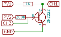
In the following schematic; the collector current can be calculated using known PV1 value and the measured CH1 value as follows;

IC = (PV1 – CH1) / 1000

This is how it is actually implemented in the existing experiments.

If one needs to implement a new experiment of any kind, these are the basics need to know. There can be so many new experiments implemented using these basics. Some of them could be;

  • Effect of Temperature coefficient in Collector current
  • The influence in β factor in Collector current

Resources:

Continue ReadingBasics behind BJT and FET experiments in PSLab

Providing Support for Performing Rectifier Experiments in PSLab Android

PSLab can be used to perform Half and Full Wave Rectifier Experiments. A rectifier is an electrical device that converts alternating current (AC), which periodically reverses direction, to direct current (DC), which flows in only one direction. Half wave rectifiers clip out the negative part of the input waveform. The rectified signal can be further filtered with a capacitor in order to obtain a low ripple DC voltage. Only a diode is needed to clip out the negative part of the input signal. Full wave rectifiers combine the positive halves of 180 degrees out of phase input waveforms such as those output from AC transformers with a center tap. The rectified signal can be further filtered with a capacitor in order to obtain a low ripple DC voltage. Two diodes are used to clip out the negative parts of both inputs and combine them into a single output which is always in the positive region.

In order to support Half Wave Rectifier Experiments in PSLab, we used Oscilloscope Activity. For Half Rectifier Experiment we require to generate a sine wave from W1 channel and read signals from CH1 and CH2.

To implement this we first need to inform the Oscilloscope Activity whether Half Wave Rectifier Experiment needs to be performed or not. For this, we used putExtra and getExtra methods.

  Bundle extras = getIntent().getExtras();
  if ("Half Rectifier".equals(extras.getString("who"))) {
          isHalfWaveRectifierExperiment = true;        
 }

Then we programmatically change the layout. The side panel is made disappear and the graph and lower panel of the Oscilloscope expands horizontally.

if (isHalfWaveRectifierExperiment) {
            linearLayout.setVisibility(View.INVISIBLE);
            RelativeLayout.LayoutParams lineChartParams = (RelativeLayout.LayoutParams) mChartLayout.getLayoutParams();
            lineChartParams.height = height * 5 / 6;
            lineChartParams.width = width;
            RelativeLayout.LayoutParams frameLayoutParams = (RelativeLayout.LayoutParams) frameLayout.getLayoutParams();
            frameLayoutParams.height = height / 6;
            frameLayoutParams.width = width;
        }

The fragment for lower panel is replaced by the fragment designed for Half Wave Rectifier

halfwaveRectifierFragment = new HalfwaveRectifierFragment();
 
if (isHalfWaveRectifierExperiment) {
addFragment(R.id.layout_dock_os2, halfwaveRectifierFragment, "HalfWaveFragment");
 }

We get the following layout, ready to perform halfwave rectifier experiment.

For making the graph functional, capturing signals from CH1 and CH2 is required. For this, we reused CaptureTwo AsyncTask in such a way that it captures signals from CH1 and CH2 channels where CH1 is the input signal and CH2 is the output signal.

if (scienceLab.isConnected() && isHalfWaveRectifierExperiment) {
   captureTask2 = new CaptureTaskTwo();
   captureTask2.execute("CH1");
   synchronized (lock) {
       try {
           lock.wait();
       } catch (InterruptedException e) {
           e.printStackTrace();
       }
   }
}


By following the above steps we reused Oscilloscope Activity to perform Rectifier Experiments.

Resources

Continue ReadingProviding Support for Performing Rectifier Experiments in PSLab Android

Electronics Experiments with PSLab

Numerous college level electronics experiments can be performed using Pocket Science Lab (PSLab). The Android app and the Desktop app have all the essential features needed to perform these experiments and both these apps have quite a large number of experiments built-in. Some of the common experiments involve the use of BJT (Bipolar Junction Transistor), Zener Diode, FET (Field Effect Transistor), Op-Amp ( Operational Amplifier) etc. This blog walks through the details of performing some experiments using the above commonly used elements.  

The materials required for all the experiments are minimal and includes a few things like PSLab hardware device, components like Diodes, Transistors, Op-Amps etc., connecting wires/jumpers and secondary components like resistors, capacitors etc. Most of these elements would be a part of the PSLab Accessory Kit.

It is recommended to read this blog here, go through the resources mentioned at the end and also get acquainted with construction of circuits before advancing with the experiments mentioned in this blog.

Half Wave and Full Wave Rectifiers

The Bipolar Junction Transistor (BJT) can be used as a rectifier. Rectifiers are needed in circuits to obtain a nearly constant and stable output voltage and prevent any ripples in the circuit. The rectifier can be half wave or full wave depending on whether it rectifies one or both cycles of Alternating Voltage.

The circuit for the Half and Full Wave rectifier is given as follows:

  • Construct the above circuits on a breadboard.
  • For the half wave rectifier, connect the terminals of CH1 and GND of PSLab on the input side and the terminals of CH2 and GND on the output side.
  • The terminals of W1 and GND are also connected on the input side and they are used to generate a sine wave.
  • Use the PSLab Desktop App and open the Waveform Generator in Control. Set the wave type of W1 to Sine and set the frequency at 100 Hz and magnitude to 10mV. Then go ahead and open the Oscilloscope.
  • CH1 would display the input waveform and CH2 will display the output waveform and the plots can be observed.
  • The plot obtained will have rectification in only half of the cycle. In order to obtain rectification in the complete cycle, the full wave rectifier is needed.
  • For the full wave rectifier, the procedure is the same but an additional diode is used. Use an additional channel CH3 to plot the extra input.

  • The plot obtained from the above steps would still have ripples and so a capacitor is placed in parallel to cancel this effect.
  • Place a 100uF/330uF capacitor in parallel to the resistor RL and an additional 1 ohm resistor in the circuit.

BJT Inverter

  • Transistor has a lot of functions. The most common of them is its use as an amplifier. However, transistor can be used as a switch in a circuit i.e. as an inverter.
  • The circuit for this experiment is shown below. For this experiment, it is recommended to use an external 5V DC supply like a battery. Connect the transistor and the diode initially and then connect the resistors accordingly. (Connect the terminals of diode and transistor carefully else they will be damaged).
  • When the circuit is constructed completely, connect CH1 to Vi and CH2 to Vo. Vi and Vo are input and outputs respectively and are marked in the figure.
  • The terminals of W1 and GND are also connected on the input side and they are used to generate a sine wave.
  • Use the PSLab Desktop App and open the Waveform Generator in Control. Set the wave type of W1 to Sine and set the frequency at 200 Hz and magnitude to 10mV.
  • Then go ahead and open the Oscilloscope. Use the X-Y mode of the oscilloscope to obtain the plot between Vi and Vo which should look like the graph shown below.

Common Mode Gain and Differential Mode Gain in Op-Amps

Gain of any amplifier can be calculated by calculating the ratio of the output and input voltage. On plotting the graph in X-Y mode, a Vo vs Vi graph is obtained. The slope of that graph gives us the gain at any particular input voltage.

  • For finding the Differential Mode gain of an Op-Amp, construct the circuit as shown below.
  • When the circuit is constructed completely, connect CH1 to Vi and CH2 to Vo. Vi and Vo are input and outputs respectively and are marked in the figure. The terminals of W1 and GND are also connected on the input side and they are used to generate a sine wave.
  • The power supply provided to the Op-Amp are set to + 12V. (If faced with any confusion, please refer to the resources mentioned at the end of the blog to learn more about Op-Amps before proceeding ahead.)
  • Use the PSLab Desktop App and open the Waveform Generator in Control. Set the wave type of W1 to Sine and set the frequency at 1000 Hz and magnitude to 0.5V. Then go ahead and open the Oscilloscope. Use the X-Y mode of the oscilloscope to obtain the plot between Vi and Vo.
  • For finding the Common Mode gain of the Op-Amp, remove the waveform generator input i.e W1 from R3 and attach it to R2. The rest of the steps remain the same.

Schmitt Trigger

In electronics, a Schmitt trigger is a comparator circuit with hysteresis implemented by applying positive feedback to the noninverting input of a comparator or differential amplifier. It is an active circuit which converts an analog input signal to a digital output signal.

  • Construct the circuit as shown below. Although the diagram shows a variable resistor be used, a constant value resistor would also work fine.
  • When the circuit is constructed completely, connect CH1 to Vi and CH2 to Vo. Vi and Vo are input and outputs respectively and are marked in the figure. The terminals of W1 and GND are also connected on the input side and they are used to generate a sine wave.
  • The power supply provided to the Op-Amp are set to + 12V. (If faced with any confusion, please refer to the resources mentioned at the end of the blog to learn more about Op-Amps before proceeding ahead. If done incorrectly, Op-Amps will be damaged)
  • Use the PSLab Desktop App and open the Waveform Generator in Control. Set the wave type of W1 to Sine and set the frequency at 1000 Hz and magnitude to 0.5V. Then go ahead and open the Oscilloscope. Use the X-Y mode of the oscilloscope to obtain the plot between Vi and Vo which should look like the graph shown below.

Resources:

  1. Read more about Half wave and Full wave rectifier and their applications – https://en.wikipedia.org/wiki/Rectifier
  2. Read more about the Bipolar Junction Transistor and its use as a switch – http://www.electronicshub.org/transistor-as-switch/
  3. Understand the common mode and differential mode of Op-Amp – https://www.allaboutcircuits.com/video-lectures/op-amps-common-differential/
  4. Find more about Schmitt Trigger and its uses – https://en.wikipedia.org/wiki/Schmitt_trigger

Continue ReadingElectronics Experiments with PSLab

Implementing Experiment Functionality in PSLab Android

Using the PSLab Hardware Device, users can perform experiments in various domains like Electronics, Electrical, Physics, School Level experiments, etc. These experiments can be performed using functionalities exposed by hardware device like Programmable Voltage Sources, Programmable Current Source, etc. In this post we will try implementing the functionality to perform an experiment using the PSLab Hardware Device and the PSLab Android App.

Let us take the Ohm’s law experiment as an example and see how it’s implement using the  PSLab Android App.

Ohm’s law states that the current through a conductor between two points is directly proportional to the voltage across the two points, effectively using a constant of proportionality called Resistance (R) where,

R = V / I

Schematic

Layout to perform Ohm’s law experiment

The Ohm’s law experiment requires a variable current, so a seekbar is provided to change the current coming from PCS channel, values of which are continuously reflected in the TextView next to it.

Implementation

The Read button has a listener attached to it. Once it is clicked, the currentValue is updated with the value parsed from the seekbar progress and the selectedChannel variable is assigned from the spinner. These variables are used by the background thread to change the current supplied by current source (PCS pin) of the device and to read the updated voltage from the selected channel of the device.

btnReadVoltage.setOnClickListener(new View.OnClickListener() {
   @Override
   public void onClick(View v) {
       selectedChannel = channelSelectSpinner.getSelectedItem().toString();
       currentValue = Double.parseDouble(tvCurrentValue.getText().toString());
       if (scienceLab.isConnected()) {
           CalcDataPoint calcDataPoint = new CalcDataPoint();
           calcDataPoint.execute();
       } else {
           Toast.makeText(getContext(), "Device not connected", Toast.LENGTH_SHORT).show();
       }
   }
});

CalcDataPoint is an AsyncTask which does all the underlying work like setting the current at the PCS channel, reading the voltage from the CH1 channel and triggering the update of the data points on the graph.

private class CalcDataPoint extends AsyncTask<Void, Void, Void> {

   @Override
   protected Void doInBackground(Void... params) {
       scienceLab.setPCS((float) currentValue);
       switch (selectedChannel) {
           case "CH1":
               voltageValue = scienceLab.getVoltage("CH1", 5);
               break;
           case "CH2":
               voltageValue = scienceLab.getVoltage("CH2", 5);
               break;
           case "CH3":
               voltageValue = scienceLab.getVoltage("CH3", 5);
               break;
           default:
               voltageValue = scienceLab.getVoltage("CH1", 5);
       }
       x.add((float) currentValue);
       y.add((float) voltageValue);
       return null;
   }

   @Override
   protected void onPostExecute(Void aVoid) {
       super.onPostExecute(aVoid);
       updateGraph();
   }
}

updateGraph() method is used to update the graph on UI thread. It creates a new dataset from the points which were added by the background thread and refreshes the graph with it using the invalidate() method.

private void updateGraph() {
   tvVoltageValue.setText(df.format(voltageValue));
   List<ILineDataSet> dataSets = new ArrayList<>();
   List<Entry> temp = new ArrayList<>();
   for (int i = 0; i < x.size(); i++) {
       temp.add(new Entry(x.get(i), y.get(i)));
   }
   LineDataSet dataSet = new LineDataSet(temp, "I-V Characteristic");
   dataSet.setColor(Color.RED);
   dataSet.setDrawValues(false);
   dataSets.add(dataSet);
   outputChart.setData(new LineData(dataSets));
   outputChart.invalidate();
}

Roadmap

We are planning to add an option to support multiple trials of the same experiment and save each trails for further reference. App flow to perform experiment is based on Science Journal app by Google.

Resources

  • Article on Ohm’s law and Power on electronics-tutorial
  • To know more about Voltage, Current, Resistance and Ohm’s law, head on to detailed tutorial on sparkfun
  • Implementation of perform experiment functionality in PSLab Desktop App

Continue ReadingImplementing Experiment Functionality in PSLab Android